witec360 Semicon
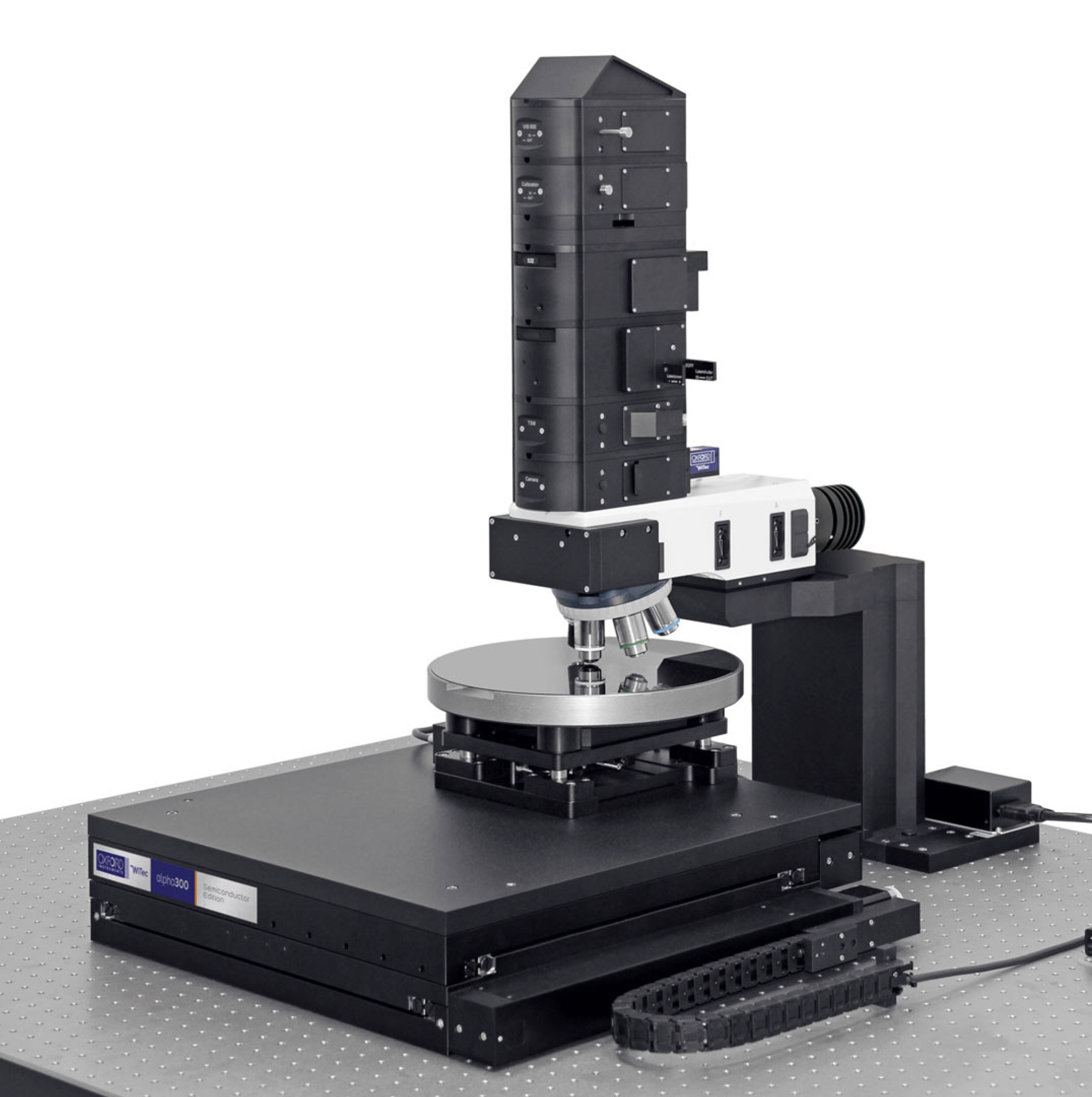


witec360 Semicon
Large-area analysis of wafers in the semiconductor industry
The witec360 Semiconductor Edition is a high-quality confocal Raman and photoluminescence microscope that has been specially configured for the chemical imaging of semiconductor materials. It helps researchers to accelerate the characterisation of crystal quality, strain and doping in their semiconductor samples and wafers.
The microscope’s scanning stage covers a particularly large area, enabling the examination of entire wafers with diameters of up to 300 mm (12 inches) as well as the acquisition of large-area Raman images. The instrument features vibration damping and active focus stabilisation to compensate for topographical variations during long or large-area measurements. Full automation of all components enables the instrument to be controlled remotely and allows recurring measurement processes to be defined.
- Complete inspection of wafers up to 300 mm (12 inches)
- Non-destructive characterisation of crystallinity, polymorphism, defects, residual stresses and doping
- Analysis of wide-bandgap and multilayer semiconductors
- Surface analysis, depth scans and 3D imaging
We are looking forward to hearing from you